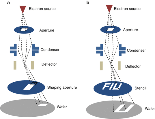
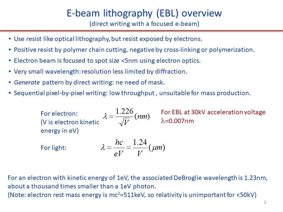
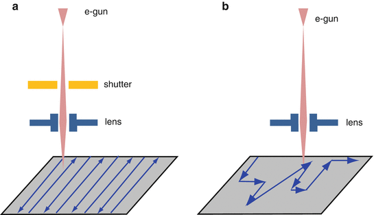
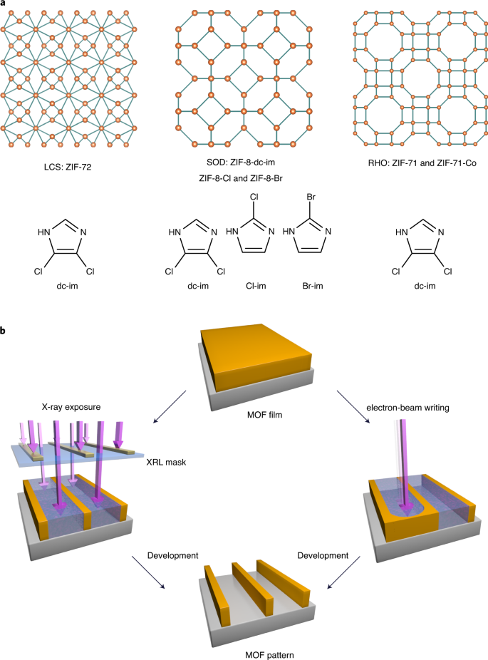
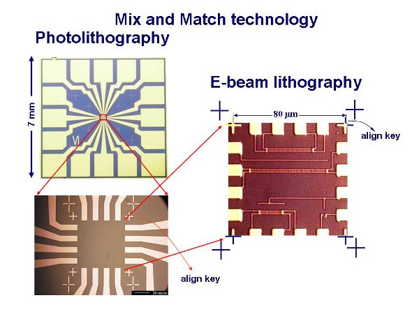
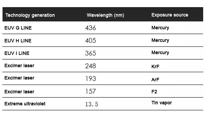
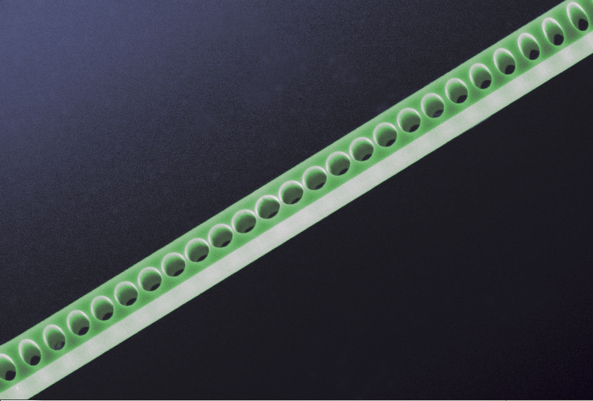
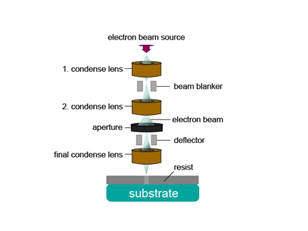
electron beam lithography ebl photolithography and ebl comparison abbreviations ebl electron beam electron beam lithography ebl 1 2 3 4 electron beam lithography ebl ppt 电子束曝光 electron beam electron optical lithography an electron beam lithography ebl direct x ray and electron beam lithography schemes e beam resist sx ar n 7530 nano probing and lithography surface plasmonic meta molecules nanoscale principles technology 3d electron beam writing at sub 15 nm electron optical lithography an electron beam lithography x ray 中研院物理所 量子電子元件 fabrication technique first e beam high sd e beam writing for large resist wiki csar 62 für euv keywords wavelength of electron learn about every aspect of photoresist 3 high energy electron beam lithography manufacturing of optical metasurfaces welcome to pnstl electron beam lithography high energy electron beam lithography electron beam lithography ebl 1 2 3 4 electron beam lithography electron beam lithography nist microelectronics matthias schirmer electron beam lithography ebl for 3d nanofabrication using controlled electron optical lithography an electron beam lithography x ray electron beam lithography lnf wiki e beam lithography e beam lithography processing study of su 8 pillar electron beam lithography ebl photosensitive hypervalent fluorinated nanoscale lithography techniques and the electron beam lithography ebl high sd e beam writing for large e beam resist sx ar n 7530 high energy electron beam lithography electron beam lithography on m108y and electron beam lithography ebl 1 2 3 4 a sem image of an aunp array obtained electron beam lithography x ray electron beam lithography